

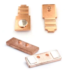
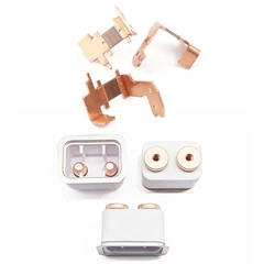

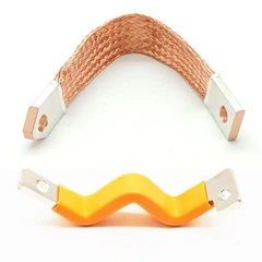


Precision Stamping Techniques for High-Conductivity Copper and Beryllium Copper Parts
Oct 02, 2026
Leave a message
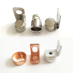
C1100 copper provides electrical conductivity up to 100% IACS, while beryllium copper combines high conductivity with substantially higher spring strength after precipitation hardening. For conductive springs, clips, terminals, and contact components, material temper, strip thickness, forming radius, springback compensation, and aging treatment must be controlled as one stamping process rather than as separate operations.
For high-current paths, the design target is low electrical resistance; for spring-loaded contacts, it is stable contact force after repeated deflection. This creates a different engineering requirement for OEM production of copper stamping parts than for conventional carbon-steel stamping.

C1100 Copper vs BeCu: Conductivity, Strength and Spring Performance
C1100 Copper - 100% IACS Conductivity for Low-Resistance Stamping
C1100 is commercially pure copper with electrical conductivity commonly specified around 100% IACS. It is suitable for busbar connectors, conductive terminals, current-carrying clips, and stamped electrical components where conductivity has priority over mechanical strength.
The main limitation is mechanical behavior. Annealed or soft copper is highly ductile but has limited spring retention. Cold-worked copper improves hardness and strength, but excessive work hardening can increase forming load and reduce dimensional stability during subsequent operations.
Typical engineering considerations include:
C1100 / 100% IACS: low electrical resistance for high-current paths.
Cold-worked strip: higher hardness and yield strength than annealed material.
Tight bend radii: require verification against material temper and thickness.
Spring elements: require controlled deformation rather than simply maximum hardness.
Stamping tolerance: ±0.01 mm may be achievable on selected critical dimensions after DFM review.
BeCu - High Conductivity with Spring-Grade Mechanical Strength
Beryllium copper is selected when a stamped component must simultaneously conduct current and maintain elastic force. After solution treatment, quenching, and precipitation aging, BeCu can achieve significantly higher hardness and strength than pure copper while retaining useful electrical conductivity.
This combination makes beryllium copper stamping parts suitable for:
Electrical contact springs
Connector terminals
Battery and power-electronics contact clips
Relay and switch components
Shielding springs
High-cycle electrical contacts
Precision conductive clips
The engineering trade-off is straightforward: increasing alloy strength through precipitation hardening normally reduces conductivity compared with C1100. Material selection therefore starts from the required current, contact force, working deflection, and thermal conditions rather than from conductivity alone.
| Property / Design Factor | C1100 Pure Copper | BeCu Alloy | Engineering Implication |
| Electrical conductivity | Up to ~100% IACS | Lower than C1100, grade dependent | C1100 favors low-resistance current paths |
| Spring strength | Low to moderate | High after aging | BeCu favors contact springs |
| Work hardening | Significant | Significant | Forming sequence affects final properties |
| Precipitation aging | Not applicable | Required for precipitation-hardened grades | Heat-treatment process must be controlled |
| Formability | Excellent in soft temper | Depends strongly on temper | Radius and forming sequence require DFM |
| Contact-force retention | Limited in soft temper | High after proper aging | BeCu is suitable for repeated deflection |
| Typical application | Busbars, terminals, conductive clips | Springs, terminals, precision contacts | Select according to electrical + mechanical load |
C1100 and BeCu Selection Under IEC 60269 and High-Current Design Requirements
For fuse-related and power-distribution components, electrical performance must be considered together with the applicable product standard, temperature rise, and contact resistance. Where components form part of a fuse system, the finished assembly may be evaluated against IEC 60269, while the stamped component itself requires material and dimensional controls appropriate to its function.
For automotive applications, production approval and traceability may additionally require IATF 16949 quality systems and PPAP documentation.
Request Free DFM Evaluation & Quote

±0.01 mm Springback Control in Precision Copper Stamping
Springback Is a Material-and-Geometry Problem, Not Just a Die Problem
Copper and BeCu strip have different elastic recovery characteristics depending on alloy, temper, thickness, grain direction, and forming geometry. A nominal 90° bend in CAD therefore does not necessarily produce a 90° stamped angle.
For precision high-conductivity metal stamping, springback compensation must be established from measured production data.
Important variables include:
Material temper: changes yield strength and elastic recovery.
Strip thickness: affects bending moment and forming force.
Bend radius: smaller radii increase local strain.
Grain direction: can influence bend behavior and cracking risk.
Forming sequence: earlier bends can alter subsequent geometry.
Coining: locally reduces elastic recovery through controlled plastic deformation.
Over-bending: compensates for predictable springback.
Tool wear: changes forming geometry over long production runs.
±0.01 mm Tolerance Requires Feature-Based Process Control
Not every dimension on a stamped copper component should be assigned ±0.01 mm. Reserve tight tolerance for functional interfaces such as connector mating features, terminal positioning, contact spacing, and critical assembly datums.
A practical inspection structure can include:
| Feature | Control Method | Typical Engineering Target |
| Critical linear dimension | CMM / optical measurement | ±0.01 mm where specified |
| Bend angle | Optical / CMM | Drawing-specific |
| Material thickness | Micrometer | Material specification |
| Burr height | Optical measurement | Drawing-specific |
| Hole diameter | Pin gauge / CMM | Drawing-specific |
| Flatness | CMM / height measurement | Drawing-specific |
| Contact position | CMM | ±0.01 mm where required |
| Plating thickness | XRF | Supplier specification |
Burr Control for Electrical Contact Geometry
A burr on a high-current terminal can create several problems: reduced mating area, local stress concentration, coating damage or interference during assembly.
For electrical contacts, the stamping direction should therefore be considered during product design. Critical contact surfaces should be positioned with the required edge condition in mind rather than relying on post-stamping deburring as the primary correction.
For copper stamping parts OEM production, progressive dies can integrate controlled piercing, forming, coining, and in-die riveting while minimizing secondary handling.

Precipitation Hardening and Aging Control for BeCu Spring Contacts
Solution Treatment, Quenching and Aging Under Controlled Thermal Profiles
BeCu achieves its high mechanical performance through precipitation hardening. The process generally consists of solution treatment, rapid cooling, and subsequent aging.
The metallurgical sequence can be simplified as:
Solution treatment → Quenching → Forming → Aging → Final inspection
However, the exact thermal cycle depends on alloy grade, strip condition, thickness, and required mechanical/electrical properties. A production process should therefore use the material supplier's approved heat-treatment window rather than applying a generic temperature-time recipe.
Why Aging Changes Contact Performance
A BeCu contact spring is not specified only by hardness. The finished component must maintain a stable force under repeated deflection.
The relationship can be expressed conceptually as:
Contact Force ≈ Material Elastic Modulus × Geometry × Deflection
If precipitation aging changes yield strength, the allowable elastic working range also changes. Over-aging can reduce strength; under-aging can leave the component below the required hardness and spring-force specification.
For this reason, production controls should include:
Material heat number and certificate traceability
Alloy and temper verification
Furnace temperature uniformity
Time-at-temperature recording
Cooling/quenched condition
Hardness verification
Electrical conductivity verification
Dimensional inspection after heat treatment
Contact-force testing where specified
Conductivity and Mechanical Strength Must Be Balanced
| Requirement | C1100 | BeCu After Aging | Design Consideration |
| Conductivity | Up to ~100% IACS | Grade-dependent | C1100 has the electrical advantage |
| Elastic strength | Lower | High | BeCu supports spring contacts |
| Permanent deformation resistance | Moderate | High | BeCu favors repeated loading |
| Thermal treatment | Normally not precipitation-aged | Solution + aging | Heat-treatment control required |
| Spring-contact suitability | Application-dependent | High | Particularly useful for compact contacts |
For automotive electrical systems, the finished component should be validated under the actual temperature, current, and mechanical cycling conditions specified by the customer drawing or component specification.
Progressive Die Design for IATF 16949 Precision Production
Progressive Stamping Combines Piercing, Forming and In-Die Riveting
A progressive die moves strip stock through multiple stations while maintaining a controlled material reference. A typical conductive terminal may use:
Coil feeding → Pilot positioning → Piercing → Notching → Coining → Bending → Forming → In-die riveting → Parting
The actual station sequence depends on component geometry and material condition.
For high-volume beryllium copper stamping parts, progressive tooling provides repeatability while reducing manual handling between operations.
Strip Layout Controls Material Utilization and Part Stability
The strip layout should balance three factors:
Material utilization
Carrier rigidity
Forming stability
An aggressive material-utilization target can reduce scrap but may weaken the carrier between stations. For thin copper strip, insufficient carrier width can cause strip deformation during high-speed feeding.
Pilot holes and carrier geometry therefore need to be evaluated together with feed pitch, press accuracy, and forming loads.
In-Die Riveting for Conductive Contact Assemblies
Where a silver contact or another conductive insert is required, in-die riveting can integrate mechanical joining into the progressive stamping sequence.
Key controls include:
Rivet height
Rivet head diameter
Contact position
Base-material thickness
Riveting force
Contact seating
Burr formation
Pull-off or shear strength
This approach can reduce secondary assembly operations and improve positional repeatability.
Tool Wear and Production Stability Under IATF 16949
Copper alloys can generate different friction and galling behavior from carbon steel. Tool material, coating, clearance, lubrication, and maintenance intervals therefore affect dimensional consistency.
A production control plan should identify wear-sensitive features such as:
Piercing punches
Fine blanking edges
Forming radii
Coining surfaces
Pilot pins
Riveting punches
For automotive programs, IATF 16949, process FMEA, control plans, MSA, and PPAP documentation provide the framework for managing these variables.
Progressive Die Clearance for C1100 and BeCu High-Conductivity Stamping
Punch-to-Die Clearance Determines Burr, Edge Quality and Tool Life
Copper alloys require clearance selection based on alloy, temper, thickness, and cutting geometry. Excessive clearance can increase rollover and burr formation; insufficient clearance can increase cutting force and accelerate punch or die wear.
Rather than applying one fixed clearance percentage to every copper component, tooling engineers should establish the cutting condition through material-specific trials.
A controlled validation should examine:
| Parameter | Inspection Focus | Production Risk |
| Punch-to-die clearance | Cut-edge profile | Excessive burr/tool load |
| Strip thickness | Incoming material | Dimensional variation |
| Material temper | Hardness/certificate | Cutting-force variation |
| Punch edge condition | Microscopic inspection | Burr growth |
| Die wear | Dimension trend | Progressive tolerance drift |
| Feed accuracy | Pilot alignment | Hole-to-form positional error |
CMM and SPC Detect Dimensional Drift Before Assembly Failure
For production volumes requiring stable dimensional output, first-piece inspection alone is insufficient. Critical dimensions should be monitored through statistical process control.
A practical measurement loop is:
First Article → MSA → SPC sampling → CMM verification → Tool maintenance → Corrective action
The measurement system itself should be validated before using capability data for process decisions.
Material Selection Matrix for Copper Stamping Parts OEM Projects
Select the Alloy From Electrical, Mechanical and Process Requirements
A procurement specification should not simply state "copper stamping." The material designation, temper, thickness, conductivity requirement, mechanical requirement, and surface treatment should be explicitly defined.
| Requirement | C1100 | BeCu | Recommended Evaluation |
| Maximum electrical conductivity | Strong | Moderate to high, grade-dependent | C1100 |
| High spring force | Limited | Strong | BeCu |
| Repeated contact cycling | Application-dependent | Strong | BeCu |
| High-current busbar | Strong | Usually unnecessary | C1100 |
| Precision contact spring | Limited in soft temper | Strong | BeCu |
| High-speed progressive stamping | Suitable | Suitable with correct temper | DFM validation |
| Post-form heat treatment | Usually unnecessary | May be required | BeCu process route |
| Automotive PPAP | Available | Available | Customer-specific |
The final material choice should be based on the complete load case rather than conductivity alone.
For example, a flat current-carrying terminal may benefit from C1100 because its primary requirement is low resistance. A compact connector spring that must retain contact force after thousands of deflection cycles may justify BeCu despite its lower conductivity.
Surface Treatment and Contact Resistance Under ISO 14001 and Electrical Reliability Requirements
Plating Must Match the Contact Environment
Copper and BeCu stamping components can receive nickel, tin, silver, or other surface treatments depending on electrical, corrosion, and mating requirements.
For contact applications, plating thickness and substrate preparation directly affect contact resistance and long-term interface stability.
Typical inspection methods include:
XRF coating-thickness measurement
Cross-section metallography
Adhesion testing
Visual surface inspection
Contact-resistance testing
Salt-spray testing where specified
Thermal cycling where specified
Environmental management can also be incorporated under ISO 14001, while restricted-substance requirements may require RoHS and REACH compliance documentation.
Engineering Validation for High-Conductivity Metal Stamping
Electrical and Mechanical Validation Must Be Tested Together
A conductive spring can pass a dimensional inspection while failing its electrical or mechanical requirements. Conversely, a component can meet conductivity requirements but lose contact force after thermal cycling.
A validation program should therefore correlate:
Material → Stamping → Heat Treatment → Surface Treatment → Assembly → Electrical Test → Mechanical Test
Depending on the component, validation may include:
Contact resistance
Current-carrying capacity
Temperature rise
Contact force
Deflection cycling
Tensile/shear strength
Hardness
Electrical conductivity
Plating thickness
Dimensional stability
Corrosion resistance
Thermal cycling
For automotive programs, PPAP documentation can include dimensional results, material certifications, process capability studies, MSA, control plans, and process FMEA according to customer requirements.
OEM Production Route for C1100 and BeCu Stamped Components
From DFM Review to PPAP Level 3 Documentation
A controlled OEM production workflow can be structured as follows:
2D/3D drawing review - identify functional datums, tolerances, and material requirements.
DFM analysis - evaluate bend radii, springback, piercing, carrier design, and stamping direction.
Material confirmation - verify alloy, temper, thickness, and certificate.
Progressive die development - establish strip layout and station sequence.
T1 sampling - verify dimensions and forming behavior.
Tool correction - compensate measured springback and dimensional deviations.
Process validation - establish stable production parameters.
CMM / optical inspection - verify critical dimensions.
Electrical and mechanical testing - validate application-specific requirements.
PPAP Level 3 submission - provide customer-required production approval documentation.
Mass production - monitor critical dimensions through SPC and scheduled tooling maintenance.
This route is particularly relevant when a Tier 1 customer requires traceability from incoming copper strip through final stamped contact components.
Design Checklist for High-Conductivity Copper and BeCu Components
IATF 16949 DFM Checklist for Precision Stamping
Before releasing a drawing for tooling, engineering and procurement teams should verify:
Material designation and temper are specified.
Copper conductivity requirement is defined in % IACS.
BeCu hardness or mechanical requirement is defined after aging.
Critical dimensions are separated from general tolerances.
Bend radius is compatible with material temper.
Springback compensation is included in the tooling strategy.
Burr direction is considered at functional contact edges.
Plating thickness is specified where applicable.
Contact resistance requirements are defined.
Heat-treatment requirements are documented for BeCu.
CMM inspection datums are included.
Progressive-die carrier geometry is manufacturable.
Tool-maintenance criteria are defined.
PPAP requirements are agreed upon before mass production.
FAQ
What is the typical PPAP Level 3 delivery cycle for copper stamping parts?
A typical PPAP Level 3 schedule depends on drawing complexity, progressive-die design, T1 corrections, and customer documentation requirements. The production sequence normally includes DFM, tooling, T1 sampling, dimensional validation, and final PPAP submission.
How can BeCu stamping parts maintain spring force after repeated deflection?
BeCu achieves high spring retention through controlled precipitation hardening. Solution treatment, quenching, and aging must be controlled against the specified alloy and temper, followed by hardness, conductivity, and contact-force verification.
How is ±0.01 mm tolerance verified on precision copper stamping parts?
Critical ±0.01 mm dimensions can be verified using CMM, optical measurement, or calibrated gauges, depending on geometry. The drawing must define functional datums, measurement method, and acceptance criteria before production.
Request Free DFM Evaluation & Quote
contact us

Send Inquiry