



High-Current Copper Busbars and Contact Solutions for Commercial Energy Storage (BESS)
Sep 27, 2026
Leave a message
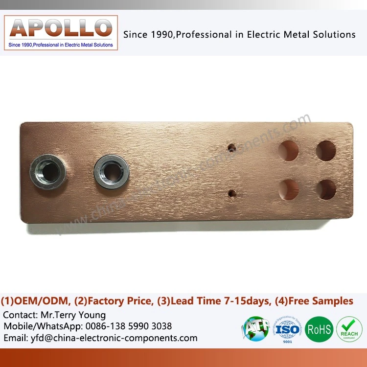
For commercial and industrial BESS, the DC busbar system must carry high continuous current while controlling oss, temperature rise, dielectric clearance, and mechanical stress. C1100 high-purity copper provides high electrical conductivity; silver-plated contact surfaces reduce interface resistance, while laminated insulation and controlled bending geometry support 1000V+ DC applications.
The electrical connection system is not simply a copper strip. A production-ready BESS assembly requires material selection, stamping tolerance, joint resistance, welding quality, insulation integrity, dimensional inspection, and traceable quality control to remain within the electrical and thermal limits of the PCS and battery architecture.
1000V+ DC BESS Current Paths Require Controlled Resistance and Heat
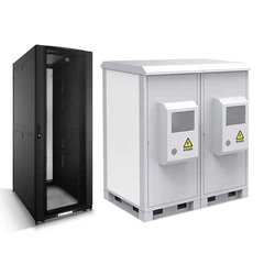
Commercial energy storage systems commonly contain battery racks, DC combiner units, DC contactors, fuses, pre-charge circuits, PCS interfaces, and high-current distribution paths. Each connection introduces electrical resistance.
That is why a BESS electrical contact part cannot be evaluated based only on nominal copper thickness. You must consider the entire current path, including the busbar material, contact interface, plating, joint method, bolt interface, weld zone, and thermal dissipation.
1000A Current Path Design Parameters for IEC 61439 and IEC 60664 Applications
C1100 copper: typically selected where high electrical conductivity is required; conductivity can approach 100% IACS depending on material condition.
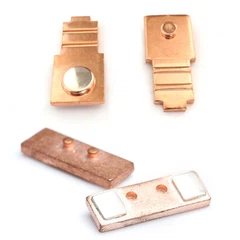
Silver-plated interfaces: used to reduce contact resistance and improve resistance to oxidation at electrical interfaces.
Laminated busbar insulation: controls phase-to-phase and phase-to-ground dielectric separation.
CMM dimensional inspection: verifies hole position, bending geometry, and critical tolerances.
IEC 60664 insulation coordination: provides the framework for clearance and creepage evaluation.
IEC 61439 assemblies: relevant where busbar systems are integrated into low-voltage power assemblies.
C1100 Copper vs. C2680 Brass for High-Current Energy Storage Connections
| Parameter | C1100 Pure Copper | C2680 Brass |
| Typical electrical role | Main current path | Mechanical/electrical components |
| Conductivity | Up to ~100% IACS | Significantly lower than pure copper |
| Electrical resistance | Low | Higher |
| Current-carrying application | Busbars, terminals, connectors | Terminals, brackets, stamped hardware |
| Formability | Good | Very good |
| Thermal conductivity | High | Lower |
| Typical BESS use | High-current DC distribution | Structural/contact components |
For a high-current energy storage copper busbar, C1100 is generally preferred when electrical resistance and thermal rise dominate the design constraints. C2680 can remain appropriate where forming strength, wear resistance, or mechanical geometry has greater influence.
Silver-Plated C1100 Interfaces Control Contact Resistance Under 1000A+ DC Loads
Copper provides the bulk current path, but the interface between two conductive components can become the local thermal bottleneck.
Oxidation, insufficient contact pressure, surface contamination, poor flatness, and inconsistent plating thickness can increase contact resistance. Under high current.
3–12 μm Silver-Plating Control for IEC 60269 and DC Contact Applications
For BESS electrical contact parts, surface treatment may include:
Silver plating: commonly used on high-current electrical contact interfaces.
Nickel underlayer: may be used as a diffusion barrier depending on the material stack.
3–12 μm coating range: selected according to electrical, mechanical, and environmental requirements.
Plating-thickness verification: performed using appropriate coating-thickness measurement equipment.
Contact-resistance testing: evaluates the completed interface rather than relying solely on material conductivity.
Visual and microscopic inspection: identifies plating discontinuity, burns, peeling, cracks, or exposed substrate.
The correct plating specification should be established from current density, contact force, mating cycles, environmental exposure, and required service life rather than using a universal thickness.
In-Die Riveting and Resistance Silver Brazing for BESS Contact Assemblies
| Joining Method | Main Advantage | Main Process Risk | Typical Application |
| In-die riveting | High repeatability and short cycle time | Rivet height and clinching consistency | Contact assemblies |
| Resistance silver brazing | Conductive metallurgical joint | Heat input and brazing-layer control | Copper/contact assemblies |
| Laser welding | Localized heat input | Reflectivity and weld penetration | Cu-Cu or Cu-Al structures |
| Bolted connection | Serviceable joint | Torque relaxation and interface resistance | Busbar installation |
For production volumes requiring repeatable contact geometry, in-die riveting integrates component forming and joining into a controlled stamping sequence. For permanent conductive joints, resistance silver brazing can provide a metallurgical connection when joint clearance, temperature, filler distribution, and surface condition are controlled.
Request Free DFM Evaluation & Quote
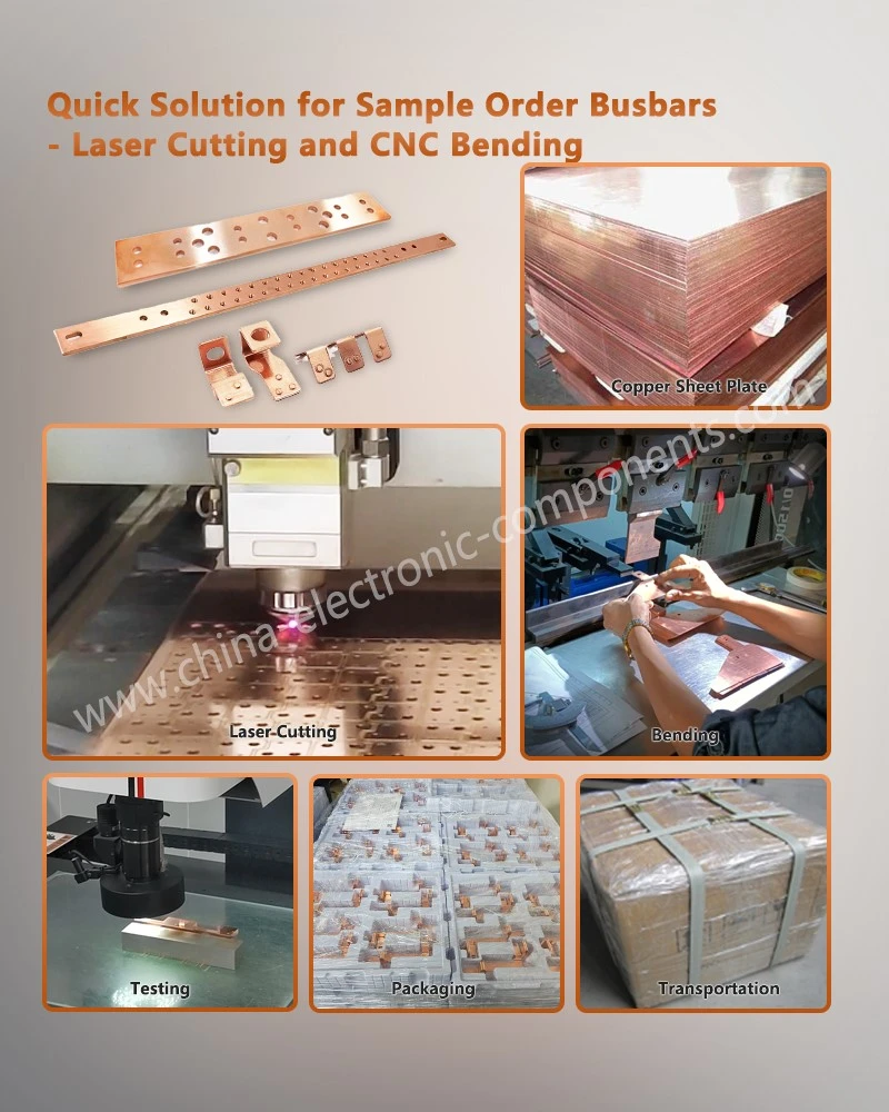
Laminated Busbars for 1000V+ DC Insulation and Controlled Inductance
A conventional bare copper bar provides current capacity but does not inherently solve insulation, electromagnetic coupling, or installation geometry.
A laminated busbar combines conductive layers with an insulating dielectric system. In high-frequency switching environments, reducing conductor loop area can also reduce parasitic inductance.
For fast-switching PCS architectures, a compact laminated structure can support lower stray inductance. In demanding power-electronics designs, engineering targets may reach <10 nH stray inductance, but the actual value depends on conductor spacing, geometry, length, dielectric structure, and measurement method.
1000V+ DC Laminated Busbar Design Under IEC 60664 and UL 94 V-0
Key design variables include:
Conductor thickness: determined by continuous current, peak current, temperature rise, and allowable voltage drop.
Insulation thickness: selected according to working voltage, dielectric strength, creepage, clearance, and environmental conditions.
Dielectric strength: some engineered insulation systems can exceed 15 kV/mm, subject to material grade and test method.
UL 94 V-0: applicable where flame-retardant polymer performance is specified.
Creepage distance: affected by pollution degree, material group, operating voltage, and installation environment.
Bending radius: must prevent copper cracking, insulation damage, and residual mechanical stress.
Epoxy Powder Coating vs. Heat-Shrink Insulation for 1000V+ DC Busbars
| Parameter | Epoxy Powder Coating | Heat-Shrink Tubing |
| Insulation coverage | Conformal coating | Tubular |
| Complex geometry | Good when coating process is controlled | Limited by tube geometry |
| Edge coverage | Process dependent | Can leave local geometry constraints |
| Mechanical protection | High | Moderate |
| Thickness control | Controlled by coating process | Determined by tubing specification |
| High-volume automation | Suitable | Suitable |
| UL 94 V-0 option | Available for specified materials | Available for specified materials |
| Application | Laminated/bent busbars and formed parts | Straight or moderately complex conductors |
For formed BESS busbars, coating thickness must be controlled around holes, corners, bends, and terminal interfaces. Excess coating can interfere with assembly tolerances, while insufficient coverage can reduce dielectric margin.
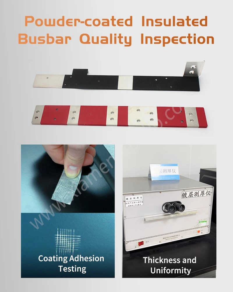
Precision Copper Stamping Under IATF 16949 and PPAP Level 3 Control
The electrical performance of a BESS copper busbar depends heavily on dimensional consistency.
A stamping component with incorrect hole position can introduce assembly stress. Excessive burr height can damage insulation or create an electrical clearance risk. Bending deviation can shift the busbar against a housing or neighboring conductor.
±0.01 mm Dimensional Control with CMM and Progressive Die Stamping
A controlled stamping process should address:
±0.01 mm critical dimensional tolerance, where required by drawing and process capability.
Progressive die stamping: integrates blanking, piercing, forming, bending, and other operations.
Tool wear monitoring: prevents progressive dimensional drift during long production runs.
Burr-height control: reduces assembly and insulation damage risk.
CMM inspection: verifies three-dimensional geometry against CAD/drawing datums.
SPC monitoring: identifies process drift before nonconforming batches accumulate.
PPAP Level 3: supports customer approval with dimensional, material, process, and capability documentation.
Copper Stamping and Bending Defects Affecting BESS Electrical Connections
| Defect | Typical Cause | Engineering Effect | Control Method |
| Excessive burr | Tool wear or incorrect clearance | Insulation damage | Die maintenance + inspection |
| Hole-position deviation | Die misalignment | Assembly interference | CMM + SPC |
| Copper cracking | Excessive forming strain | Electrical/mechanical failure | Bend-radius optimization |
| Springback | Material condition and tooling | Terminal misalignment | Compensation in die |
| Surface scratches | Material handling | Plating/coating defects | Protective handling |
| Warpage | Uneven forming stress | Poor assembly contact | Flatness inspection |
For automotive and energy-storage supply chains, process approval should not stop at a first-article sample. The control plan must connect drawing characteristics to tooling, inspection frequency, reaction plans, and traceability.
Download Busbar Design Specification
Laser Welding Cu-Al and Molecular Diffusion Welding for Low-Resistance Joints
BESS current paths increasingly combine copper and aluminum because of weight, cost, and system architecture requirements. Joining dissimilar metals introduces additional metallurgical constraints.
Copper has high thermal conductivity and high reflectivity at common laser wavelengths. Aluminum has a different melting point, thermal conductivity, and coefficient of thermal expansion. Excessive heat input can generate intermetallic compounds or defects in the transition zone.
Laser Welding Cu-Al Under Controlled Heat Input and Metallographic Inspection
A production welding window should control:
Laser power
Welding speed
Beam diameter
Focal position
Shielding gas
Joint gap
Surface condition
Copper-to-aluminum overlap
Weld penetration
Heat-affected zone
Intermetallic layer formation
The objective is not simply visual weld appearance. Cross-sectional metallography should verify penetration, fusion profile, porosity, cracking, and the condition of the Cu-Al interface.
Cu-Al Laser Welding vs. Molecular Diffusion Welding
| Parameter | Laser Welding Cu-Al | Molecular Diffusion Welding |
| Heat input | Localized | Controlled pressure/thermal process |
| Joint geometry | Flexible | Requires suitable contact surfaces |
| Production speed | High potential | Process dependent |
| Dissimilar-metal control | Requires strict heat-input window | Strong interface control |
| Metallurgical inspection | Cross-section required | Interface inspection required |
| Typical use | Battery/terminal structures | High-reliability conductive transitions |
For high-current DC assemblies, joint resistance should be measured on the completed component. A visually acceptable weld is not sufficient evidence of electrical performance.
BESS Electrical Contact Parts Connect Battery Racks, DC Contactors and PCS
A commercial energy storage system contains several electrically and mechanically different connection points.
Typical components include:
Energy storage copper busbar: distributes high DC between battery modules, racks, contactors, fuses, and PCS.
Laminated busbar: combines current conduction and controlled insulation within a compact structure.
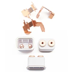
DC contactor component energy storage: includes conductive terminals, copper carriers, magnetic/structural components, and contact assemblies.
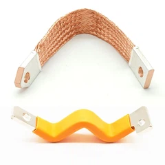
Flexible copper connector: absorbs installation tolerance and vibration-related displacement.
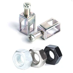
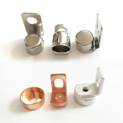
Precision copper stamping part: provides terminals, brackets, conductive links, and structural electrical components.
Silver contact assembly: controls the electrical interface in switching devices.
The engineering specification should define the electrical role of each component instead of applying one generic copper-busbar specification to the complete system.
BESS Electrical Connection Matrix Under IEC 60664 and IATF 16949
| System Position | Primary Requirement | Typical Material/Process |
| Battery module interconnect | Low resistance + compact geometry | C1100 stamping/bending |
| Rack DC bus | High current + thermal control | C1100 copper busbar |
| DC contactor terminal | Low interface resistance | Copper + silver plating |
| PCS DC input | Current capacity + insulation | Laminated busbar |
| Fuse connection | Low resistance + mechanical retention | Stamped copper/brass |
| Flexible connection | Vibration absorption | Laminated/flexible copper |
| Cabinet distribution | Electrical spacing + mechanical rigidity | Formed/insulated busbar |
BESS Supplier Quality Control: CMM, Resistance, Dielectric and Burst Testing
For an energy-storage component supplier, dimensional inspection and material certification are only part of the quality system.
A production control plan should link incoming material, stamping, welding, plating, insulation, assembly, and final testing.
IATF 16949 and ISO 14001 Manufacturing Control Points
IATF 16949: process quality management for automotive-related production environments.
ISO 9001: quality management and documented process control.
ISO 14001: environmental management system requirements.
CMM inspection: three-dimensional dimensional verification.
Plating-thickness testing: confirms specified surface-treatment thickness.
Contact-resistance testing: verifies electrical interface performance.
Dielectric withstand testing: evaluates insulation integrity.
Insulation resistance testing: detects leakage paths.
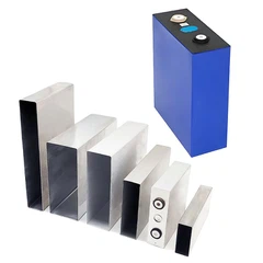
Burst pressure test: applicable to pressure-containing battery or cooling-related structures where specified.
PPAP Level 3: provides structured production-part approval documentation.
Typical BESS Component Validation Sequence
Material verification → Stamping inspection → Welding inspection → Plating verification → Insulation inspection → Dimensional CMM → Electrical resistance test → Dielectric test → Final assembly inspection → PPAP documentation
The sequence should be adapted to the actual component and customer drawing. Not every busbar requires every test.
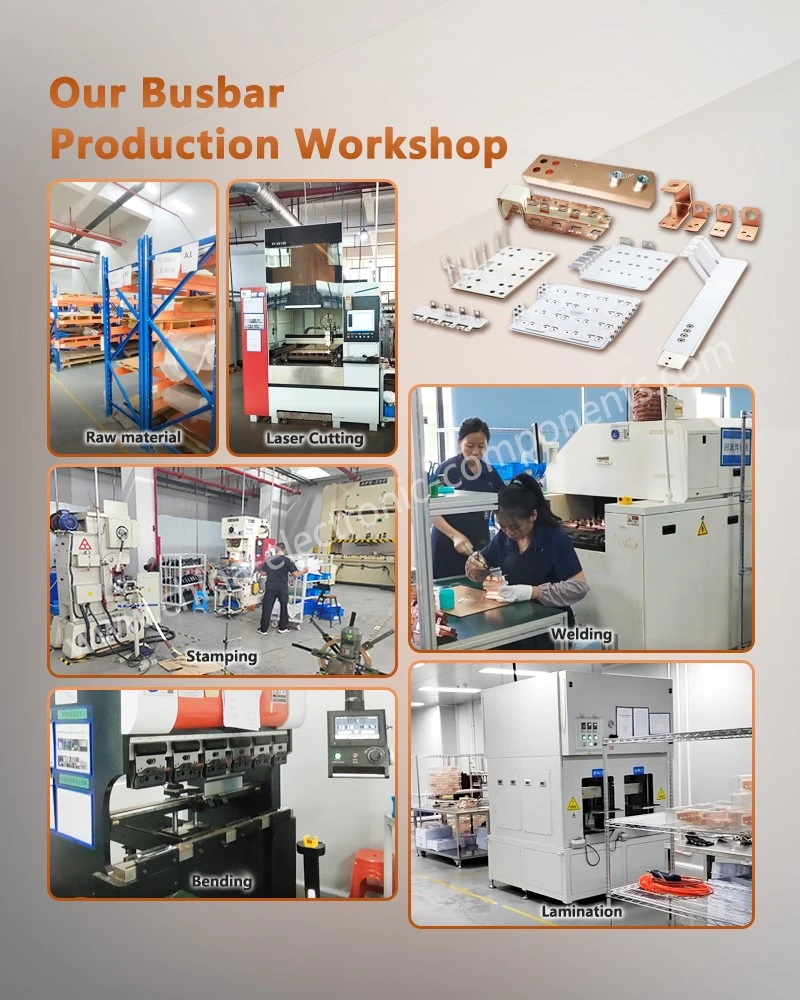
Engineering Specification Checklist for Energy Storage Copper Busbar OEM Production
Before tooling begins, the customer drawing should define the parameters that directly affect electrical, thermal, mechanical, and insulation performance.
Drawing Data Required for IEC 60664 and PPAP Level 3 Review
Material: C1100, C10200, C2680, aluminum alloy, or customer-specified grade.
Copper conductivity: target value or IACS requirement.
Thickness: nominal material thickness and tolerance.
Plating: silver, nickel, tin, or other surface treatment.
Plating thickness: specified range and measurement method.
Critical dimensions: tolerance such as ±0.01 mm where applicable.
Bending angle: tolerance and datum reference.
Hole diameter: tolerance and positional tolerance.
Flatness: maximum permitted deviation.
Burr height: maximum allowable value.
Insulation: material, thickness, dielectric requirement, and flame rating.
Working voltage: including continuous and transient conditions.
Test voltage: dielectric withstand requirement.
Contact resistance: maximum allowable value where applicable.
Welding requirements: penetration, joint geometry, and metallographic acceptance criteria.
Packaging: surface protection and anti-oxidation requirements.
Traceability: lot, material, tooling, process, and inspection records.
A clear engineering drawing reduces interpretation during DFM, tooling design, sample approval, and mass production.
From Prototype to Mass Production: Tooling, T1 Samples and PPAP Level 3
The production route for a precision copper component normally progresses through engineering review, DFM, tooling, T1 sampling, dimensional correction, process validation, and PPAP.
T1 Sample and PPAP Level 3 Production Flow
Drawing review - electrical, mechanical, material, tolerance, and inspection requirements are identified.
DFM analysis - stamping direction, bend sequence, material utilization, burr direction, and tool structure are reviewed.
Progressive die design - forming stations are arranged according to the required geometry.
T1 sampling - initial parts are produced for dimensional and functional evaluation.
Tool correction - springback and dimensional deviations are compensated.
Process validation - stamping, welding, plating, and insulation parameters are locked.
Capability verification - critical dimensions are monitored using SPC/CMM.
PPAP Level 3 submission - documentation supports customer production approval.
Mass production - approved parameters become controlled production conditions.
For high-volume copper stamping, tooling life should be established through actual material thickness, alloy hardness, stroke rate, cutting clearance, forming load, lubrication, and maintenance data rather than using an unsupported universal cycle number.
Engineering Selection Matrix for Commercial BESS Current Connections
The correct current-connection architecture depends on current, voltage, available installation space, thermal limits, switching frequency, insulation requirements, and assembly method.
500A–1000A+ BESS Busbar Selection Under IEC 60664 and UL 94 V-0
| Design Requirement | Recommended Direction | Main Engineering Check |
| High continuous DC | C1100 copper busbar | Temperature rise + voltage drop |
| Compact PCS connection | Laminated busbar | Inductance + insulation |
| High-current switching interface | Silver-plated copper/contact assembly | Contact resistance |
| Cu-Al transition | Laser welding or diffusion joining | Metallographic interface |
| Complex 3D geometry | Precision stamping + forming | Springback + CMM |
| High dielectric requirement | Epoxy insulation system | Dielectric withstand |
| High-volume production | Progressive die stamping | Tool life + SPC |
| Automotive-grade approval | IATF 16949 process | PPAP Level 3 |
For a complete BESS electrical connection system, material conductivity, joint resistance, insulation performance, mechanical tolerance, and thermal behavior must be evaluated together.
What a Qualified BESS Copper Busbar Manufacturer Should Provide
A production supplier should be able to connect the engineering specification to measurable manufacturing controls.
IATF 16949 and PPAP Level 3 Supplier Deliverables
Material certificates for copper and alloy substrates
Plating specification and thickness records
Progressive die and tooling DFM feedback
T1 sample dimensional report
CMM inspection data
Welding process parameters
Weld cross-section or metallographic reports where required
Contact-resistance test data
Dielectric withstand test records
Insulation-resistance results
SPC and capability records for critical characteristics
PPAP Level 3 documentation
Production traceability
Corrective-action records for nonconforming parts
For Apollo Electronic Components (Xiamen) Co., Ltd., the manufacturing scope can cover precision metal stamping, copper components, electrical contact assemblies, welding, surface treatment, and high-voltage/new-energy electrical connection applications. This enables the busbar and associated contact components to be reviewed as one current-path system rather than as isolated stamped parts.
FAQ
How long does PPAP Level 3 approval take for a BESS copper busbar?
The timeline depends on tooling complexity, T1 sample results, customer documentation requirements, and validation testing. A typical project proceeds through DFM, tooling, T1 sampling, dimensional correction, process validation, and PPAP submission.
What copper material is suitable for a 1000A+ energy storage copper busbar?
C1100 high-purity copper is commonly selected for high-current busbars because of its high electrical conductivity and thermal conductivity. Final selection depends on current, temperature rise, geometry, mechanical requirements, and surface treatment.
How is silver-plating thickness verified on BESS electrical contact parts?
Silver-plating thickness is verified using an appropriate coating-thickness measurement method and recorded against the specified range. Contact-resistance testing should additionally verify the completed electrical interface.
contact us
Send Inquiry