

Fabrication of Alumina Metallized Ceramic Substrates: From Process Optimization to Performance Breakthroughs
Apr 07, 2026
Leave a message
Against the backdrop of rapid development in power electronics, 5G communications, and new energy vehicles, electronic devices are continuously evolving towards higher frequencies, higher power densities, and higher reliability. As a core carrier material, the substrate not only needs excellent electrical insulation properties but also must consider thermal management capabilities and mechanical stability. In this context, Alumina Metallized Ceramics has gradually become an important technological path in the high-end packaging field, achieving synergistic optimization of performance and structure through the effective combination of ceramics and metals.

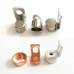
Alumina ceramics themselves possess high dielectric strength and good thermal conductivity, but direct bonding between them and metal materials presents problems such as poor interfacial wettability and mismatched coefficients of thermal expansion. Therefore, the metallization of alumina ceramics has become a key step in achieving reliable electrical interconnection. By constructing a stable metal transition layer, the overall connection strength and conductivity of the structure can be effectively improved.
From a process perspective, the current mainstream method focuses on tape casting and high-temperature co-firing techniques. Through precise control of the powder system and metallization slurry, composite structures with high density and high bonding strength are achieved. In this process, the performance indicators of Metallized Ceramics for Electrical Components typically include low dielectric loss, high insulation resistance, and excellent interfacial bonding strength. These parameters directly determine the reliability and lifespan of the final device.

Regarding the raw material system, high-purity alumina powder (typically ≥96%) combined with sintering aids can significantly improve the densification process and reduce sintering defects. Simultaneously, the selection of metallized slurry needs to be optimized according to the application scenario. For example, silver systems are suitable for high-frequency signal transmission, while copper systems are more suitable for high-power conductivity scenarios. This differentiated design of material systems is a key factor in achieving performance stratification in Alumina Metallized Ceramics for Electronic Applications.
Cast casting, as a core preparation step, hinges on the uniformity of slurry dispersion and the precision of thickness control. By optimizing the binder ratio, solvent system, and ball milling parameters, a green ceramic tape structure with low surface roughness and uniform thickness can be obtained. This type of structure provides the foundation for subsequent multilayer stacking processes and is also an important prerequisite for achieving Precision Metallized Ceramics.
In the metallization pattern construction process, screen printing remains the mainstream solution. High-precision screens and stable printing parameters enable micron-level line resolution. Subsequently, multilayer lamination and hot pressing processes form a dense composite preform structure. This process places extremely high demands on alignment accuracy and interlayer bonding, directly impacting the reliability of Alumina Metallized Ceramics for Bonding.
The high-temperature co-firing stage is a critical control point in the entire fabrication process. By properly setting the debinding curve and sintering temperature, problems such as bubbles, delamination, and internal residual stress can be effectively avoided. Especially in copper systems, sintering must be completed in a reducing atmosphere to prevent metal oxidation, thereby ensuring the structural integrity and conductivity stability of High-Strength Metallized Ceramic Components.
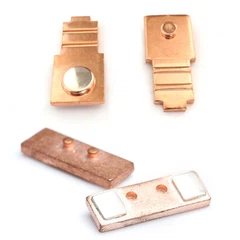
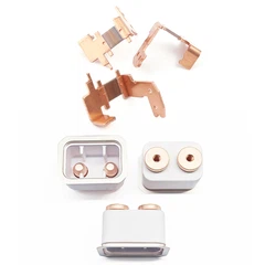
Post-processing is equally important. Precision grinding and laser processing enable high-precision shape control. Simultaneously, nickel-gold plating further improves solderability and corrosion resistance, making the product suitable for harsher industrial environments. This type of process is widely used in high-end packaging applications such as Metallized Ceramic Housing for Power Semiconductors. In actual production, insufficient interfacial adhesion, substrate warping, and bubble defects are the main technical challenges. These problems can be significantly improved by increasing raw material purity, optimizing particle size matching, and introducing segmented debinding and temperature field control technologies. Furthermore, advanced powder coating technology also helps improve interfacial reaction efficiency, thereby optimizing the overall stability of alumina metallization.
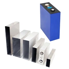
From an industrialization perspective, this technology has significant application value in new energy vehicles, power modules, and high-frequency communication equipment. For example, in high-voltage electric drive systems, ceramic substrates need to withstand both high voltage and high temperature shocks, while in the radio frequency field, higher requirements are placed on dielectric loss and signal integrity. Therefore, Metallized Ceramics for Electrical is gradually replacing traditional substrate materials and becoming one of the key supporting technologies.

In the future, alumina metallized ceramic substrates will develop towards ultra-thinness, multi-layer integration, and multi-functional integration.
Simultaneously, the introduction of nanoscale metal pastes, digital process simulation, and environmentally friendly water-based systems will further promote improvements in manufacturing precision and sustainability. These development trends will continue to deepen the application of Metalized Ceramic Insulating Tubes and Metalized Ceramic Parts in high-end electronics.
Furthermore, ultrasonic spraying is gradually becoming an important auxiliary process in advanced packaging technologies. Compared to traditional spin coating and dip coating, it can achieve more uniform thin film deposition and high coverage of complex surface structures, making it particularly suitable for coating microstructure devices. The introduction of this technology provides greater process flexibility and precision assurance for the precision machining of alumina ceramic parts.
About Us
In the field of precision electronic packaging and electrical connections, we focus on the research, development, and manufacturing of high-performance ceramic and metal composite structures, continuously optimizing alumina metallization processes and precision machining capabilities.
Around the requirements of high reliability and high consistency, we have formed a product system covering various structural forms and application scenarios, providing stable material solutions for power devices, communication equipment, and new energy systems. By continuously improving process control capabilities and material matching levels, we are committed to providing customers with more competitive high-end ceramic metallized components.
contact us

Send Inquiry