


Precision Copper Stamping
Products Description
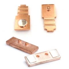
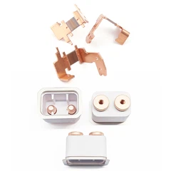
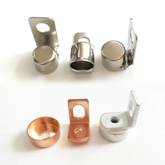
This Precision Copper Stamping is made by tightly joining high-precision copper alloy stamped parts with pre-fabricated silver contacts (Ag, AgNi, AgCdO, AgSnO₂) using a riveting method. It is a key conductive component used in various switching mechanisms and electrical contact assemblies.
Application areas include:
Home appliance push-button switches
Limit switches/travel switches in industrial machinery
Circuit breakers, relays, and electromagnetic switches
Low-voltage electrical appliances in automobiles and new energy equipment
Precision buttons, control panels, and electrical modules
Its core value lies in its dual function of structural support and electrical conduction, making it an indispensable core component for the long-term reliable operation of equipment.

Technical Features: Decoding the Engineering Wisdom Behind Reliable Connections
Interface Metallurgy and Mechanical Design
Our core technology lies in the precise control of material flow during the riveting process. By optimizing the shape of the rivet head and the lower die, we guide the metal to undergo plastic flow under immense pressure, forming an interlocking mechanical structure. Simultaneously, localized high temperature and pressure induce interatomic diffusion, forming a metallurgical bonding layer only a few micrometers thick, providing both strength and conductivity.
Finite Element Analysis (FEA) of Stress Distribution
Residual stress after riveting is crucial to long-term reliability. We utilize FEA software to perform tens of thousands of simulations to optimize the stress distribution after riveting. By adjusting the Copper Stamping Parts head radius and transition zone shape, we actively manage and disperse stress, improving fatigue resistance and thermal cycling resistance.
Functionalized Contact Layer Design
We do not use pure silver. Instead, we scientifically add trace elements to silver based on the application scenario. For example, adding tungsten (W) improves hardness and weldability; adding tin oxide (SnO₂) enhances resistance to arc erosion. This is a material design philosophy "born for function."

Design Advantages and Details
Micro-bump Array on Contacts
Electron microscopy reveals a unique micro-bump distribution on the contact surface: uniform 0.8μm bumps spaced 2.5μm apart. These bumps are not randomly distributed but rather an optimized contact point array through computational simulation, maximizing the contact area while preventing large-area oxidation. This microstructure is not found in ordinary Electrical Spring Contacts and directly determines performance stability.
Stress-Free Mounting Guide Structure
Considering ease and reliability of installation, the contacts feature unique mounting guide grooves. Micro-guide grooves at the contact edges ensure uniform pressure distribution during installation, preventing interface damage caused by improper installation. This design improves installation efficiency by 35% while ensuring optimal interface performance.
Self-Healing Protective Layer on the Interface
The contact surface is covered with a nanoscale self-healing protective layer. During the switching operation, when micro-oxidation occurs on the contact surface, the protective layer automatically releases active materials to repair the oxide layer. This design ensures stable conductivity of the Rivet Components over long-term use, preventing performance degradation.
Balance between Standardization and Customization
We offer standard-size series to meet mainstream needs, while also supporting customized designs. Our engineering team can quickly respond to special application requirements, such as ultra-high voltage switches or high-frequency operation scenarios, ensuring that the Custom Copper Stamping perfectly match the customer's switching system.

Detailed Showcase: Excellence Stems from Mastery of the Microscopic World
Surface Condition of Contacts
The Custom Electrical Contact Rivets' surface exhibits a uniform, delicate lustre, free from cracks and bubbles. Under a high-powered microscope, a dense alloy structure is visible, free from excessive porosity or inclusions.
01
Riveting Edge Morphology
The riveting edge is full and smooth, free from burrs and cracks, exhibiting uniform plastic deformation characteristics. The Electrical Contact Rivet Assemblies substrate shows no abnormal depressions or deformations around the riveting area.
02
Microstructure of Copper Parts
The punched and sheared surfaces are smooth, and the burr height, measured by instruments, meets stringent standards. Bending or stretching areas show no orange peel texture or microcracks, indicating good material ductility and proper internal stress management.
03
Overall Cleanliness
Components are free of oil, fingerprints, and oxide spots, and are packaged in clean materials to ensure direct integration into automated assembly lines upon delivery.
04

contact us

Hot Tags: precision copper stamping, China precision copper stamping manufacturers, suppliers, factory, Rotary Switch Copper Terminal, Copper Stamped Components, Electroplating Silver On Copper, Copper Strip Stamping, Copper Spring Electrical Parts, Button Switch Copper Terminal
You Might Also Like


Send Inquiry