



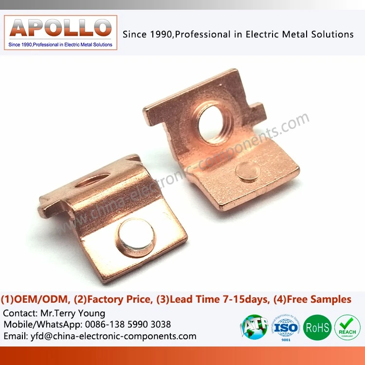
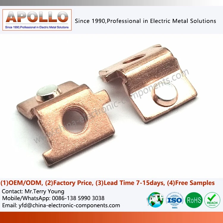
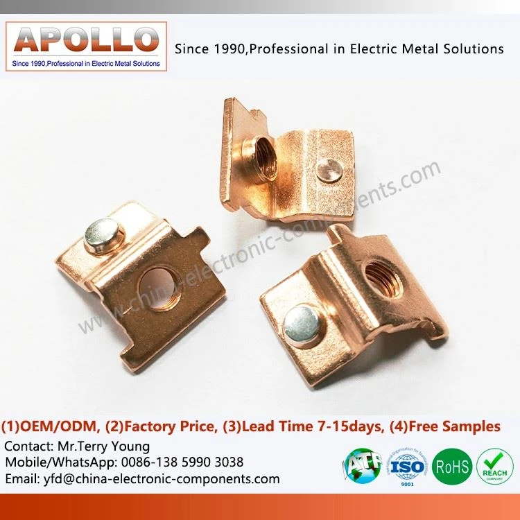
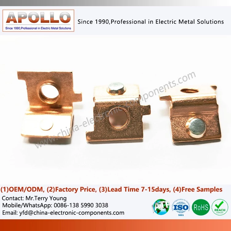
Copper Electrical Stamping
Products Description

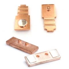
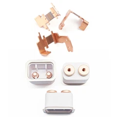
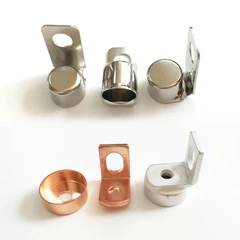
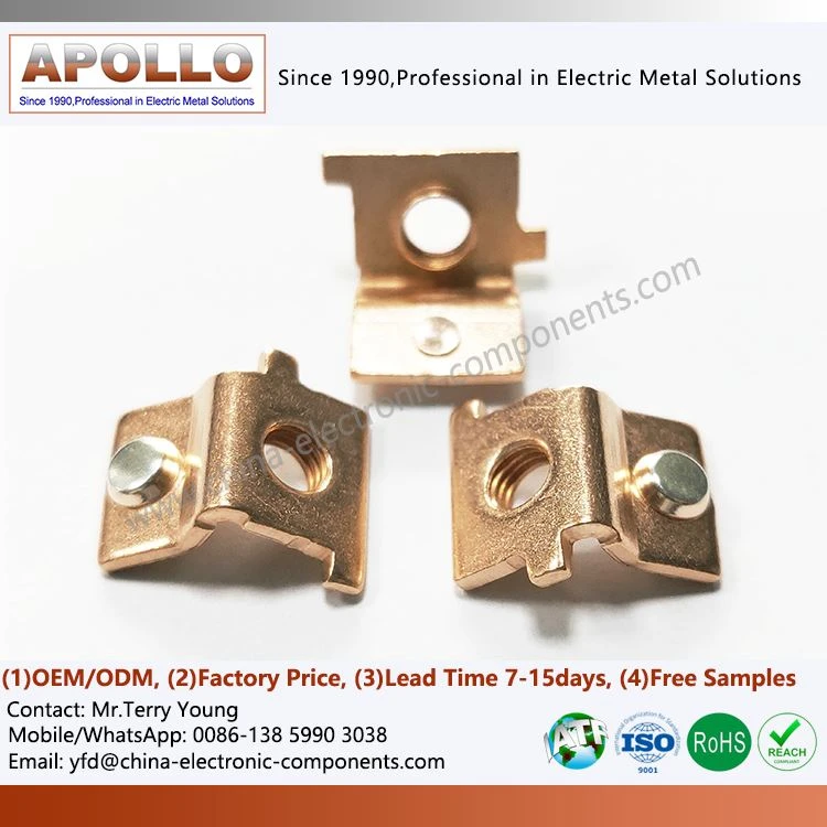
Copper Electrical Stamping is a functional metal component made from highly conductive copper using precision moulds and high-speed stamping technology. It possesses the following fundamental properties:
Precise Conductivity: Low material resistance ensures stable and reliable current transmission.
Precise Dimensional Control: Meets the stringent tolerance requirements of electronic and electrical structures.
Moderate Mechanical Strength: Combining flexibility and strength, suitable for snap-fit, crimping, and embedding structures.
Mass Production Capability: Automated stamping achieves highly consistent output.
Multi-Process Composite Manufacturing: Includes bending, punching, edging, welding, and plating.
Suitable for Multi-System Integration: Electrical modules, connectors, busbar terminals, battery modules, etc.
In-depth Technical Analysis – The Physical Essence of Stamping
| Active Guidance and Control of Metal Flow | Precision stamping is not simply "punching," but rather the active guidance of metal flow. Through draw beads, undulating structures, and local blank holder force control in the die, we guide the material to flow along the designed path, ensuring uniform thickness distribution and avoiding excessive thinning or material accumulation in certain areas. This flow control capability determines the mechanical strength and electrical uniformity of the product. |
| The Electrical Significance of Edge Quality | The sheared edge quality of stamped parts is often underestimated, but its impact on electrical performance is significant. Rough edges increase resistance, generate hot spots, and accelerate oxidation. Our Precision Copper Stamping technology can achieve smooth sheared surfaces with a bright band ratio of over 90%, and edges that are virtually burr-free and tear-free. For high-frequency applications, we further employ chemical or electrochemical polishing to reduce edge roughness to the microscopic level, minimising skin effect losses. |
| Directed Evolution of Microstructure | The stamping process alters the microstructure of copper: grains are elongated, dislocation density increases, and texture changes. We not only accept these changes but also guide them in a favourable direction through process design. For example, in contact areas requiring high elasticity, we design specific strain paths to create a reinforcing texture; in areas requiring high conductivity, we control the degree of deformation to preserve the large grain structure. This "microstructure engineering" allows us to achieve differentiated local properties within the same Copper Stamping Supplier. |

Material Advantages: Unleashing the True Value of Copper
Material Design Addresses Core Industry Pain Points:
Purity Advantage: 99.99% electrolytic copper (Cu-ETP) ensures conductivity ≥98% IACS, far exceeding brass (70% IACS)
Grain Advantage: Oriented grains form low-resistance paths, reducing electron scattering
Environmental Advantage: 100% recyclable material, reducing the carbon footprint of the production process by 40%
Cost Advantage: High-purity copper costs only 5% more than brass, but offers 3 times better performance.
These material advantages extend Copper Metal Stamping Service lifespan by 2.2 times in high-temperature and high-humidity environments, while avoiding electrochemical corrosion caused by alloying elements.

Wide Range of Applications: Ubiquitous as a Cornerstone
Connectors and Terminals
As the "interface" for data and power transmission, our high-precision terminals ensure connection reliability and signal integrity.
01
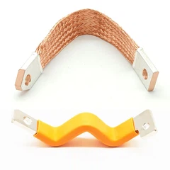
Buses and Busbars
Copper Progressive Stamping In power systems and new energy modules, our customised buses handle massive current distribution with minimal resistance.
02
EMI/RFI Shielding
In communication equipment and precision instruments, our shielding covers create an impenetrable barrier against electromagnetic interference for sensitive circuits.
03
LED Heatsink Brackets and Substrates
In the lighting field, our stamped parts serve as both the carrier of LED chips and a channel for efficient heat dissipation, directly determining the lifespan and luminous efficacy of lamps.
04
Automotive Electronics and Sensors
In the harsh automotive environment, our stamped parts provide stable Copper Electrical Stamping connections and structural support for ECUs, sensors, and actuators.
05

contact us

Hot Tags: copper electrical stamping, China copper electrical stamping manufacturers, suppliers, factory, Button Switch Copper Terminal, Rotary Switch Copper Terminal, copper terminal, Precision Copper Stamping Parts, Copper Strip Stamping, Electroplating Silver On Copper
You Might Also Like


Send Inquiry