

Alumina Ceramic Metallization Technology Drives Innovation in The Fields Of New Energy And High-voltage Electrical Equipment.
Jun 13, 2026
Leave a message
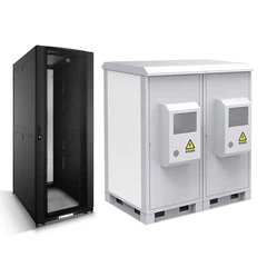
With the rapid development of new energy vehicles, energy storage systems, rail transit, and industrial automation equipment, the demand for high-reliability insulating materials continues to grow. As a key representative of advanced ceramic materials, alumina ceramics, with their excellent insulation properties, high-temperature resistance, and mechanical strength, have become an indispensable basic material in the electronics and electrical industries. In recent years, technological innovations surrounding the metallization of alumina ceramics have continuously advanced, bringing new development opportunities to the fields of high-voltage relays, HVDC contactors, and power semiconductor packaging.

Alumina ceramics can be divided into two main categories according to their alumina content: high-purity and ordinary. High-purity alumina ceramics typically have an alumina content exceeding 99%, possessing excellent electrical insulation properties and high-temperature resistance, and are widely used in high-end electronic devices, semiconductor packaging, and new energy power systems. Ordinary alumina ceramics, due to their good overall performance, are widely used in wear-resistant parts, electrical insulation, structural components, and industrial equipment.
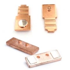
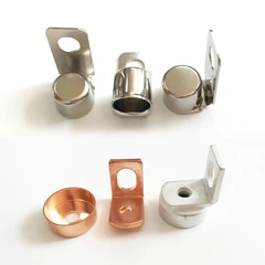
In modern electronic devices, ceramics themselves are insulating materials; therefore, their application in circuit systems often requires surface metallization. By forming a stable and robust metal layer on the ceramic surface, functions such as conductivity, welding, and signal transmission can be achieved. These types of Alumina Metallized Ceramics for Electronic Applications have become an important component of new energy vehicles, high-voltage electrical equipment, and industrial control systems.
The development of ceramic metallization technology has gone through several stages. Currently, common processes in the industry mainly include thick-film processes, direct copper bonding (DBC) processes, direct copper plating (DPC) processes, low-temperature co-fired ceramic (LTCC) processes, and high-temperature co-fired ceramic (HTCC) processes. Different processes have their own characteristics in terms of cost, conductivity, processing accuracy, and reliability.
Thick-film processes have advantages such as mature technology and suitability for high-current applications, and therefore have long been used in the manufacturing of electronic circuits and power modules. However, due to limitations in circuit accuracy, high surface roughness, and certain limitations in adhesion, their application in high-density electronic products is somewhat restricted.
DBC processes, by achieving direct bonding between the copper layer and the ceramic substrate, can achieve excellent thermal conductivity and current-carrying capacity, and are therefore widely used in the field of high-power modules. Especially in the manufacturing process of Metallized Ceramic Housing for Power Semiconductors, DBC technology can effectively improve the heat dissipation efficiency and operational stability of devices. However, due to its complex manufacturing process and high production costs, its application is relatively concentrated in the high-end market.
DPC (Digital Curve Polymer) technology, on the other hand, balances high circuit precision and good surface flatness, meeting the development needs of miniaturized electronic devices. With the rapid development of new energy vehicles and intelligent power electronic equipment, the market demand for high-precision metallized ceramics continues to grow, driving the continuous upgrading of related manufacturing technologies.

LTCC (Low-Temperature Ceramic Coating) and HTCC (High-Temperature Ceramic Coating) technologies are mainly used in the manufacture of multilayer ceramic structures. Although they can achieve complex circuit integration, they still face certain challenges in terms of dimensional control, process stability, and production costs. Therefore, in the field of high-performance electrical insulation structural components, the industry is continuously exploring more advanced solutions.
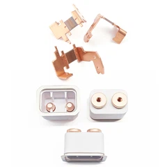
In recent years, with the development of laser processing, precision coating, and 3D forming technologies, alumina ceramic metallization processes have begun to develop towards higher precision, higher adhesion strength, and more complex structures. Especially in the high-voltage systems of new energy vehicles, key components such as EV Relay Alumina Ceramic Housing, High Voltage DC Ceramic Contactor, and HVDC Contactor High Purity Ceramics Shell For Relay place higher demands on the quality of ceramic metallization.
High-voltage DC relays and contactors need to operate stably for extended periods in environments with voltages of hundreds or even thousands of volts. Therefore, the ceramic housing must not only possess excellent insulation properties but also ensure reliable metal-to-metal connection performance. To this end, the industry widely adopts Alumina Metallized Ceramics for Bonding technology to guarantee a stable bond between the metal terminals and the ceramic structure, thereby improving overall product reliability.
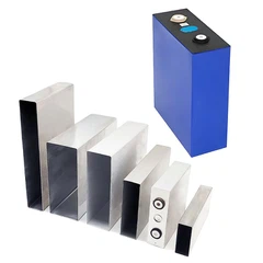
In the new energy vehicle sector, EV Alumina Ceramic Housing and Alumina Relay Ceramic Envelope for Electric Automobiles have become crucial components of high-voltage relays. These products can effectively withstand arcing, high-temperature environments, and long-term mechanical stress, providing safety assurance for battery management systems, charging systems, and drive control systems.
Meanwhile, with the advancement of intelligent manufacturing, Alumina ceramic parts' precision machining technology continues to mature, enabling ceramic structural components to achieve more complex geometries and stricter dimensional tolerances. This provides more possibilities for design innovation in high-end relays, contactors, and power electronic modules.

Currently, alumina ceramic metallization technology is widely used in Metallized Ceramics for Electrical equipment, power semiconductor modules, high-voltage relays, energy storage systems, and industrial automation control equipment. Among them, products such as High Temperature Metallized Ceramic Relay Cases and Metallized Ceramic Insulating Tubes Metalizating Ceramic Parts are gradually becoming important components of high-reliability electrical systems.
In the future, with the continued advancement of the new energy industry, high-voltage direct current transmission and distribution systems, and smart grid construction, the market demand for Metallized Alumina Ceramics for Electrical Components is expected to further increase. Higher precision, higher reliability, and more complex ceramic metallization technologies will become an important technological direction driving the upgrading of the electronics and electrical industry, providing solid support for the next generation of high-performance power electronic equipment.
contact us

Send Inquiry