
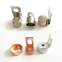

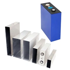

Why is pure copper, the raw material for Copper Stamping Parts, called purple copper?
May 12, 2026
Leave a message
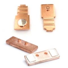
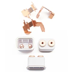
Pure copper, as one of the core raw materials in the copper stamping industry, is the preferred material for copper stamping products in electrical and mechanical manufacturing fields due to its excellent electrical and thermal conductivity and good plasticity. Many industry professionals wonder: pure copper doesn't appear purple, so why is it called "purple copper"? This naming is closely related to the surface characteristics of pure copper, and its unique material advantages make it one of the most commonly used basic materials in the Copper Stamping process.
Metallic copper is a metal with a long and crucial history of human use, widely applied in electrical, light industry, machinery manufacturing, construction, and defense industries. Because changes in copper demand directly reflect macroeconomic trends, copper prices fluctuate with economic fluctuations. Therefore, copper is also known as "Dr. Copper" by investors, serving as an important reference for predicting economic trends. The rise and fall of the Copper Stamping industry is closely related to the fluctuations in the copper market.

Pure copper is called purple copper primarily due to the color of its surface oxide film. When industrial pure copper is exposed to the atmosphere, a dense oxide film naturally forms on its surface. This film exhibits a "reddish-purple" hue, rather than the bright purple of violet. It is this purple oxide film that gives pure copper its common name, "purple copper," a characteristic clearly observable by custom copper stamping companies during processing.
Besides its name, the crystal structure and microstructure of pure copper also determine its core position in the copper stamping industry. Pure copper maintains a face-centered cubic (FCC) crystal structure at both high and low temperatures. This crystal structure gives it excellent electrical and thermal conductivity, far exceeding that of brass, bronze, and other copper alloys. This is the core reason why pure copper is widely used in electrical copper stamping products. The electrical conductivity of copper sheet stamping directly depends on the material properties of pure copper.
From a microscopic perspective, as-cast copper has an α-phase structure. When trace elements are present, it forms α-solid solutions or second-phase particles and compounds, and in severe cases, slight dendritic crystals may appear. After processing and deformation, the structure of copper changes accordingly, forming a deformed structure. This structural characteristic makes it suitable for various copper stamping processes. The precision forming of Electrical Copper Stamping Parts relies heavily on the excellent structural stability of copper.
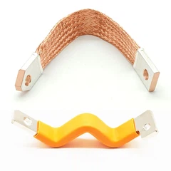
Copper has extremely excellent processing performance, which is a key reason why it is the preferred raw material for copper stamping. In industrial production, copper is almost entirely supplied as processed products. Its excellent plasticity allows for a processing rate of up to 99%, enabling multiple stamping processes to be completed without intermediate annealing, significantly improving the efficiency of copper stamping. The mass production of Metal Stamping Parts Electric Copper relies on the excellent processing performance of copper.
Copper has a low recrystallization temperature, only 200-280℃. This characteristic allows for the adjustment of material properties through annealing processes during copper stamping. When certain alloying elements are added, the recrystallization temperature of copper increases or decreases. With increasing annealing temperature and time, the recrystallized grains grow significantly, affecting the hardness and ductility of copper. The performance control of copper stamping parts largely depends on this annealing characteristic.
The most common phenomenon in the annealed microstructure of copper is annealing twins, a typical characteristic of copper's microstructure. In the face-centered cubic crystal of copper, atoms are arranged in a close-packed manner on the (111) crystal plane, while annealing twins are formed by atoms arranged symmetrically about a certain crystal plane. This microstructure further enhances the ductility and toughness of copper, meeting the requirements of high-precision stamping processes such as copper strip stamping.

In general, pure copper is called "purple copper" because of the purple oxide film formed in the atmosphere, rather than the color of its fresh surface. Its excellent electrical and thermal conductivity, superb ductility, and good processing performance make it an indispensable core raw material in the copper stamping industry, supporting the production and upgrading of Copper Sheet Stamping.
If you would like to learn more about the material properties and processing technology of pure copper, or have technical consultation or procurement needs for Copper Stamping Parts, please contact us for professional and comprehensive industry support and customized solutions.
contact us

Send Inquiry