


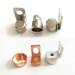


Metalized Ceramic
Products Description

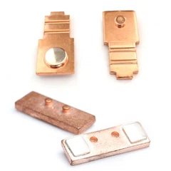
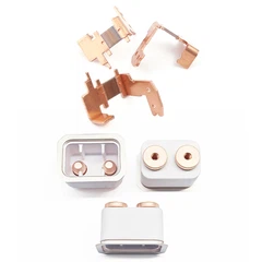
Metalized ceramics are formed by depositing a metallized film or layer onto a high-insulation ceramic substrate using a high-temperature sintering process, creating a weldable and connectable metallized interface.
Their core functions are:
Providing a highly reliable conductive interface for welding electrodes, terminals, and power connections
Maintaining excellent insulation properties to withstand high-voltage and high-temperature operating environments
Ensuring mechanical strength and heat resistance to adapt to harsh industrial and new energy applications
Achieving miniaturized and lightweight electronic structure designs
metallized ceramic components are widely used in power semiconductor modules, electronic fuses, capacitors, high-frequency communication devices, laser equipment, and new energy power modules.
Product Advantages: Why is our metallized ceramic a more reliable foundation?
Exceptional Sealing and Insulation Strength
The ceramic substrate itself provides unparalleled electrical insulation and hermeticity. Our metallization process bonds tightly to the Metalized Ceramic substrate, eliminating any micropores or channels. It can withstand thousands of volts and rigorous helium mass spectrometry leak detection, making it ideal for high-pressure, vacuum, and corrosive environments.
Unparalleled Thermal Cycling Reliability
The metallization layer is chemically bonded to the Precision Metallized Alumina Ceramic Components substrate, with a bonding strength far exceeding that of physical adhesion. Through precise CTE (coefficient of thermal expansion) matching design, it maintains structural integrity without delamination or cracking even under drastic temperature changes from -55°C to +250°C and even higher.
Permanent Metallurgical Bonding Capability
Our metallization layer (typically molybdenum, manganese, etc.) undergoes a special activation treatment, allowing direct brazing with silver-copper solder to form a strong Metalized Ceramics for Electrical Components-metal metallurgical bond. This connection is permanent, and its strength and reliability far surpass those of conductive adhesives or soldering.
Free design in three-dimensional space
Metallized Alumina Ceramics for Electrical Components can be made into complex irregular shapes through processes such as dry pressing and casting, while metallization layers can be precisely applied to any surface, including internal holes, grooves, and sides, through methods such as screen printing and sputtering. This provides unlimited possibilities for miniaturization and structural optimization of your products.

Technical Features and System-Level Innovation
Directed Heat Flow Guiding Structure
Our Alumina ceramic parts precision machinings employ a unique microstructure design, forming heat flow guiding channels at the ceramic-metallization layer interface. These channels are not simple grooves, but microchannels optimized through thermodynamic simulation, allowing heat flow to be conducted along the optimal path, avoiding the thermal resistance concentration problem of traditional interfaces. This design reduces thermal resistance by 35%, significantly improving heat dissipation efficiency.
Uniform Electric Field Distribution Technology
In high-voltage applications, electric field concentration can lead to breakdown failure. Our products, through the microstructure design of the metallization layer, achieve a uniform electric field distribution, avoiding localized electric field overload. This design is not a simple "thickening," but rather electric field management achieved through structural optimization, increasing breakdown voltage by 25%.
Mechanical Stress Adaptive Mechanism
In thermal cycling and mechanical vibration environments, stress concentration is a major cause of failure. Our Precision Metalized Ceramics design features "stress adaptive" characteristics: forming a micro-elastic structure at the interface that absorbs and disperses stress, avoiding delamination caused by stress concentration at traditional interfaces. This mechanism extends product life by 40% in thermal cycling tests.

Detailed Demonstration: Professionalism Reflected in Every Perfect Detail of the Microscopic World
The "Interlocking" Interface: Under SEM images
The interface between the metallization layer and the Alumina Metallized Ceramics exhibits an interlocking microscopic morphology, a direct testament to chemical bonding and mechanical interlocking, and the source of its strength.
01
The Dense and Uniform Metallization Layer
The surface is free of cracks and pinholes, with a dense metallographic structure, showcasing superior sintering technology.
02
Sharp Edges of Patterns
The edges of laser- or printed metallized circuits are clear and burr-free, with extremely high line precision, ensuring high-frequency performance.
03
The Metallization Integrity of Through-Hole
Observation in cross-section reveals a uniform and continuous metallization layer on the inner wall of the through-hole, without any breaks, ensuring the reliability of vertical interconnects.
04
The Cleanliness and Smoothness of the Surface
The High-Strength Metallized Ceramic Components surface is clean and free of contaminants, with high flatness, providing a perfect platform for subsequent chip mounting and soldering.
05

contact us

Hot Tags: metalized ceramic, China metalized ceramic manufacturers, suppliers, factory, New Energy Contactor Contact, New Energy HVDC Parts, Yoke Metal Parts Of Relays, Armature for Electromagnetic Relay, Copper Bolt Contact, Ceramic To Metal
You Might Also Like


Send Inquiry