




Copper Pressed Stamped Parts: The Complete Process from Basic Principles to Quality Control
Apr 02, 2026
Leave a message
Stamping, as one of the most widely used forming methods in the metal processing field, is an indispensable basic process in modern manufacturing. It uses a die and a press to apply external force to metal sheets at room temperature, causing the material to separate or undergo plastic deformation, thereby obtaining parts of the required shape and size. Whether in the automotive, electrical, home appliance, or precision electronics industries, Red Copper Stamping Parts play a crucial role in structural connection, electrical conduction, and functional realization. With the current trend of manufacturing towards higher precision and efficiency, stamping technology is also continuously upgrading towards automation and precision.
From a process principle perspective, stamping is mainly divided into two categories: separation processes and plastic deformation processes. Separation processes refer to the process where the local stress of the material exceeds its strength limit under external force, resulting in fracture and material separation, such as punching and blanking. Plastic deformation processes, on the other hand, involve permanent deformation that occurs when the material stress exceeds its yield strength but does not reach its fracture strength, including bending, drawing, and flanging. These two types of processes work together to form a complete stamping manufacturing system. This combined process is particularly common in Copper Stamping applications, enabling the one-step forming of complex structures.
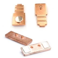
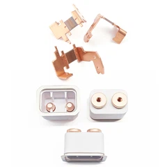
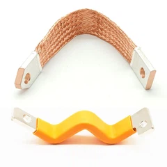
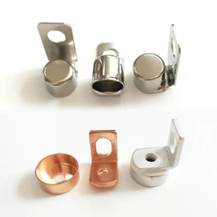
Copper-pressed stamped parts have a wide range of applications. In the automotive industry, many structural and body panels are produced using stamping processes. In the electronics industry, electrical copper stamping parts are widely used for conductive connections, switch components, and terminal structures. In home appliances and hardware products, copper stamping serves a dual role of structural support and functional implementation. Furthermore, with the development of new energy and intelligent devices, the demand for high-conductivity, high-precision custom metal copper stampings continues to grow, driving continuous industry upgrades.

Die design is a core element determining stamping quality. A well-designed die structure not only affects forming accuracy but also directly impacts production efficiency and die life. During the design process, key considerations include material flow path, clearance control, blanking force distribution, and waste removal methods. Furthermore, for the production of Copper Stamping Parts, conductivity and surface quality must be carefully monitored to avoid defects such as burrs and cracks caused by improper die design.
Stamping manufacturing offers significant advantages in cost control. A one-time investment in the die allows for large-scale, low-cost production. However, die development cycles and maintenance costs must also be comprehensively considered. Optimizing material utilization, reducing waste generation, and improving equipment utilization are key to cost reduction. These factors are particularly important in the production of Customized Copper Metal Stamping Parts in an OEM factory.
Quality inspection is crucial for ensuring the performance of Customized Electrical Stamping Copper Springs. Common inspection methods include dimensional measurement, visual inspection, hardness testing, and functional testing. For electrical Silver Plate Over Copper, conductivity and contact resistance testing are also required to ensure compliance with usage requirements. In Copper Metal Stamping Electrical Silver Contact Parts, contact quality directly impacts equipment safety, thus requiring more stringent testing standards.
Mold maintenance and upkeep are crucial for extending service life. Regularly inspecting mold wear, promptly replacing vulnerable parts, and maintaining proper lubrication effectively prevents production abnormalities. Furthermore, for high-precision Customized Metal Stamping Copper, a mold life management mechanism must be established to ensure long-term stable production.

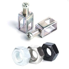
In actual production, common problems in copper connector stamping processes include burrs, deformation, dimensional deviations, and surface defects. These issues are often closely related to material properties, die design, and process parameters. For example, unevenness may stem from uneven material stress or unreasonable die pressure distribution, requiring process optimization to resolve. These problems are particularly critical to control in the manufacturing of copper connector structural components.
Overall, stamping processes are evolving towards higher precision, higher efficiency, and greater intelligence. By continuously optimizing process design, improving equipment performance, and strengthening quality control, companies can maintain their competitive edge in the fierce market. In the future, with the application of new materials and technologies, stamping manufacturing will play a vital role in more high-end fields.

contact us
For more information on Copper Spring Contacts solutions, please contact us. We will provide you with professional support and efficient service to help your projects be successfully implemented.

Send Inquiry